- 您现在的位置:买卖IC网 > Sheet目录3753 > ATMEGA169P-16MCHR (Atmel)MCU AVR 16KB FLASH 16MHZ 64-VQFN
2005 Microchip Technology Inc.
Preliminary
DS41265A-page 163
PIC16F946
13.1.4
READING THE FLASH PROGRAM
MEMORY
To read a program memory location, the user must
write two bytes of the address to the EEADRL and
EEADRH registers, set the EEPGD control bit
(EECON1<7>),
and
then
set
control
bit
RD
(EECON1<0>). Once the read control bit is set, the
program memory Flash controller will use the second
instruction cycle to read the data. This causes the
second instruction immediately following the
“BSF EECON1,RD” instruction to be ignored. The data
is available in the very next cycle, in the EEDATL and
EEDATH registers; therefore, it can be read as two
bytes in the following instructions. EEDATL and
EEDATH registers will hold this value until another read
or until it is written to by the user (during a write
operation).
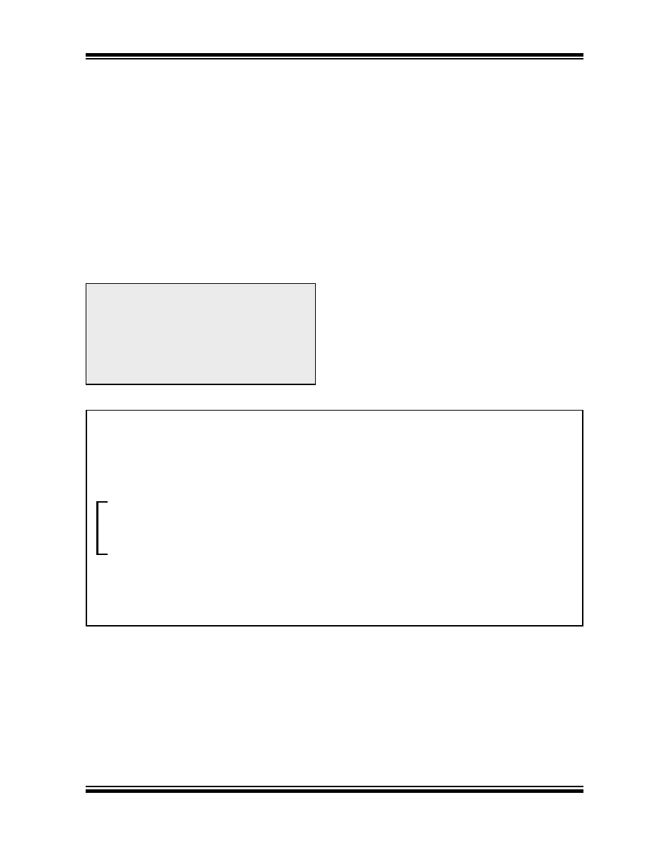
EXAMPLE 13-3:
FLASH PROGRAM READ
Note 1: The two instructions following a program
memory read are required to be NOP’s.
This prevents the user from executing a
two-cycle
instruction
on
the
next
instruction after the RD bit is set.
2: If the WR bit is set when EEPGD = 1, it
will be immediately reset to ‘0’ and no
operation will take place.
BSF
STATUS, RP1
;
BCF
STATUS, RP0
; Bank 2
MOVLW
MS_PROG_EE_ADDR;
MOVWF
EEADRH
; MS Byte of Program Address to read
MOVLW
LS_PROG_EE_ADDR;
MOVWF
EEADR
; LS Byte of Program Address to read
BSF
STATUS, RP0
; Bank 3
BSF
EECON1, EEPGD
; Point to PROGRAM memory
BSF
EECON1, RD
; EE Read
;
NOP
; Any instructions here are ignored as program
; memory is read in second cycle after BSF EECON1,RD
;
BCF
STATUS, RP0
; Bank 2
MOVF
EEDATA, W
; W = LS Byte of Program EEDATA
MOVWF
DATAL
;
MOVF
EEDATH, W
; W = MS Byte of Program EEDATA
MOVWF
DATAH
;
Re
q
u
ir
e
d
S
e
qu
en
c
e
发布紧急采购,3分钟左右您将得到回复。
相关PDF资料
2-1546217-0
TERM BLK RCPT 20POS SIDE 5.08MM
1-1546217-9
TERM BLK RCPT 19POS SIDE 5.08MM
1-1546217-8
TERM BLK RCPT 18POS SIDE 5.08MM
1-1546217-7
TERM BLK RCPT 17POS SIDE 5.08MM
1-1546217-6
TERM BLK RCPT 16POS SIDE 5.08MM
1-1546217-5
TERM BLK RCPT 15POS SIDE 5.08MM
1-1546217-4
TERM BLK RCPT 14POS SIDE 5.08MM
1-1546217-3
TERM BLK RCPT 13POS SIDE 5.08MM
相关代理商/技术参数
ATMEGA169P-16MCU
功能描述:8位微控制器 -MCU AVR 16KB, 512B EE 16MHz 1KB SRAM, 5V
RoHS:否 制造商:Silicon Labs 核心:8051 处理器系列:C8051F39x 数据总线宽度:8 bit 最大时钟频率:50 MHz 程序存储器大小:16 KB 数据 RAM 大小:1 KB 片上 ADC:Yes 工作电源电压:1.8 V to 3.6 V 工作温度范围:- 40 C to + 105 C 封装 / 箱体:QFN-20 安装风格:SMD/SMT
ATMEGA169P-16MU
功能描述:8位微控制器 -MCU AVR 16K FLASH 512B EE 1K SRAM LCD ADC RoHS:否 制造商:Silicon Labs 核心:8051 处理器系列:C8051F39x 数据总线宽度:8 bit 最大时钟频率:50 MHz 程序存储器大小:16 KB 数据 RAM 大小:1 KB 片上 ADC:Yes 工作电源电压:1.8 V to 3.6 V 工作温度范围:- 40 C to + 105 C 封装 / 箱体:QFN-20 安装风格:SMD/SMT
ATMEGA169P-16MU SL383
制造商:Atmel Corporation 功能描述:MCU 8BIT ATMEGA RISC 16KB FLASH 3.3V/5V 64PIN MLF - Tape and Reel
ATMEGA169P-16MUR
功能描述:8位微控制器 -MCU AVR LCD 16KB FLSH EE 512B 1KB SRAM-16MHZ RoHS:否 制造商:Silicon Labs 核心:8051 处理器系列:C8051F39x 数据总线宽度:8 bit 最大时钟频率:50 MHz 程序存储器大小:16 KB 数据 RAM 大小:1 KB 片上 ADC:Yes 工作电源电压:1.8 V to 3.6 V 工作温度范围:- 40 C to + 105 C 封装 / 箱体:QFN-20 安装风格:SMD/SMT
ATMEGA169P-8AU
制造商:ATMEL 制造商全称:ATMEL Corporation 功能描述:Microcontroller with 16K Bytes In-System Programmable Flash
ATMEGA169P-8MU
制造商:ATMEL 制造商全称:ATMEL Corporation 功能描述:Microcontroller with 16K Bytes In-System Programmable Flash
ATMEGA169PA
制造商:ATMEL 制造商全称:ATMEL Corporation 功能描述:8-bit Microcontroller with 16K Bytes In-System Programmable Flash
ATMEGA169PA_1
制造商:ATMEL 制造商全称:ATMEL Corporation 功能描述:High Endurance Non-volatile Memory segments